Recommended Products for This Application
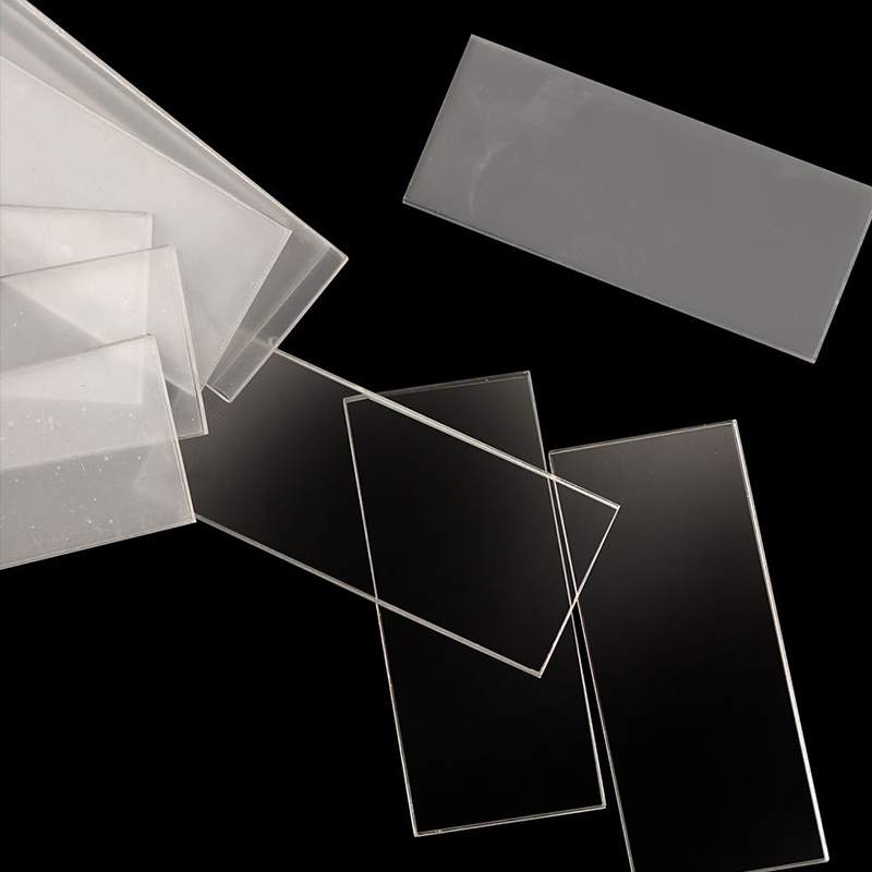
PEEK Sheet & Rod (100% Virgin)
PolyEtherEtherKetone semi-finished — black or natural, 100% virgin material for medical and industrial CNC machining.
View product →Why semiconductor fabs use PEEK (not POM) for wafer carrier components, and how to machine without contamination.
Semiconductor wet bench environments combine 80 °C+ chemistries (HF, KOH, hot DI water) with the strictest particulate cleanliness. POM, PEEK, and PFA are the three polymers that survive this regime. POM is cheaper but degrades over months of exposure. PFA is chemically perfect but soft. PEEK splits the difference: chemical resistance approaching PFA, mechanical strength approaching aluminum.
Single-wafer carriers, cassette holders, robot end-effector mounts, wet bench drying brackets. We've supplied parts for 200 mm and 300 mm wafer fabs.
Prototype 14 – 18 days. Production volume 25 – 35 days FOB Qingdao.
PolyEtherEtherKetone semi-finished — black or natural, 100% virgin material for medical and industrial CNC machining.
View product →Tell us about your high-performance engineering plastics project. Our engineering team responds within 12 hours with technical specs, lead time and a tailored quotation.